
Être bien référencé sur les moteurs de recherche, c’est formidable. C’est même ce que désire ceux, particuliers ou entreprises, qui veulent se faire connaître. Mais avoir la possibilité de se… Read more

Sous pression des autorités et de nombreuses entreprises, Apple va permettre aux éditeurs d’applications mobiles de proposer à leurs clients des moyens de paiement en dehors de l’App Store Apple… Read more

À la suite du refus de Google de supprimer des liens pointant vers des pages web contenant des données personnelles les concernant, 13 particuliers ont saisi le Conseil d’État. Tout… Read more

Les parlementaires se sont accordés en juillet dernier sur la fusion de la Hadopi et du CSA, qui formeront l’Autorité de régulation de la communication audiovisuelle et numérique (Arcom) au… Read more

C’est au Luxembourg qu’Amazon a été condamné à payer une amende de 746 millions d’euros. En raison de cette lourde sanction, des violations répétées de la réglementation de l’Union européenne… Read more

L’autorité antitrust les accuse d’avoir mis en place un « accord restrictif » qui empêchait tous les distributeurs légitimes d’opérer sur le marché. Les entreprises technologiques Amazon et Apple ont été condamnées… Read more

Le géant technologique avait refusé d’inclure dans sa plateforme une application Enel qui permet de localiser les bornes de recharge pour les voitures électriques. Le régulateur italien de la concurrence… Read more
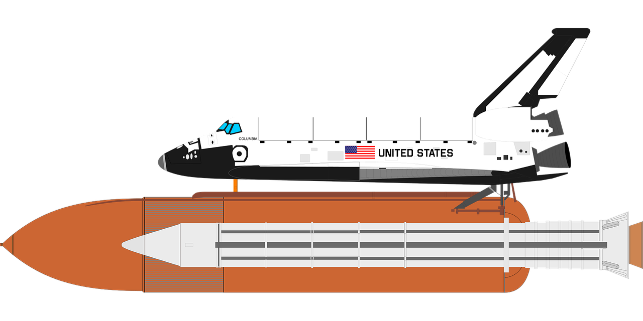
Après le triomphe de juillet, difficile retour sur Terre pour Virgin Galactic: deux mois après avoir conduit jusqu’à l’espace son flamboyant fondateur, Richard Branson, l’emblématique vaisseau de l’entreprise se retrouve… Read more

Gare aux essais de versions alternatives d’applications bien connues, mal peut vous en prendre. Encore une raison de passer sur le Play Store pour trouver vos applications. Si cette solution… Read more

L’intelligence artificielle, dans sa forme dédiée au deep learning, produit des réseaux neuronaux dotés de milliards et de milliards de paramètres neuronaux. Cette échelle croissante constitue autant de problèmes particuliers… Read more